© The Hardware Site - Fake ASUS P2B
23-05-1999
Eight ways to Identify the Counterfeit Asus P2B Mainboard.
Note: Asus P2B Mainboards with Ver. 1.02 are real Mainboards, So far we know the fake boards design follows P2B ver. 1.04.
The running models from Asus P2B are now ver 1.10 or higher.
- Fake Packaging Box.
- Fake Board Series Number.
- Fake Board Version Number.
- Fake Board PCB Script.
- Fake Board Bus Freg.Jumper.
- Fake Board CPU Slot layout.
- Fake Board Multi-I/O Layout.
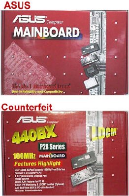
Packaging Box:
The fake boards found so far are packaed in old style gift boxes now phased-out and no longer in use from the end of Dec.1998. As picture shows here right, the fake products still use the elder box, which has been phased out since of Jan 1999. The new box is the real one that Asus now uses. You can easily distinguish.
The Real box takes away highlights list, chipset and other feature descriptions but adds two CPU's icons and MAINBOARD word. Moreover, the real one's printing is much clearer than of the fake.
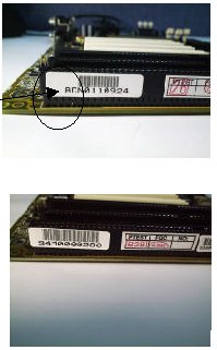
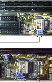
Fake Board Series Number.
First Picture is the fake board. As you can see, the series number is the same as the printed on the package box and both of them are wrong.
Second picture is the real Asus P2B Mainboard. It's series number encoding is following the rule. See Asus encoding rule which you could find on the ASUStek Web-site.
Fake Board Version Number.
First picture show the fake mainboard. On it we can see it's version is of ver. 1.04, which Asus has no longer shipped since Dec. 29th, 1998. Therefore, there should be few or none of this version in the market.
The second picture is the real Asus P2B Mainboard. It's version is of rev. 1.10 or higher, which is shipped now.
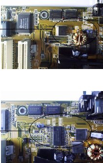
Fake Board PCB Script.
As the picture shows, beside the ASIC are some Scripts. There's not any printing words beside ASIC on real Asus P2B Mainboards
This pictures shows you the real Asus P2B Mainboard. There's no script to see on it all.
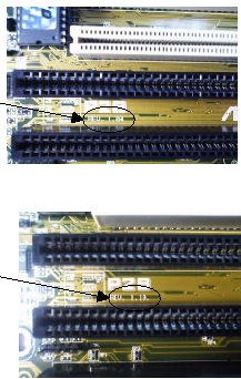
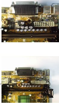
Fake Board Bus Freq. Jumper.
This picture shows the fake board. The Most outstanding difference we can see is that the bus frequency jumpers are only three in number. The real board has four on board. Moreover the layout near the clock generator is different, for example, there should still be another jumper beside the the DIMM slot.
This Picture show the real Asus P2B Mainboard. You can see that there are five jumpers located on the board. What's more, there are an AGP Frequency jumper and three lines beside the Dimm slot describing how to adjust the jumper to co-work with the system. Note: Rev 1.02 has 3-jumpers.
Fake Board CPU Slot layout
This picture shows the fake Mainboard. The Layout around the CPU Slot is different, arrangement of capacitors, compared with the real board, is obviously different.
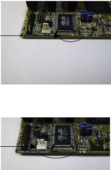
Fake Board Multi-I/O Layout
In this picture we can see the layout of a fake board around Multi-I/O Chip
And it is a little different from the real Asus P2B Mainboard.
The most obvious difference is the location of the jumper.
The real Asus P2B Mainboard and you can see the V I/O Jumper's location on the board.